
Microcontroller Kits
Programmer and Target 89s51
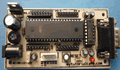
Simple Mikrokontroller 89s51 Trainer

Standart
Mikrokontroller 89s51 Trainer

Super Mikrokontroller Trainer 89s51
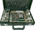
+
All Item Include
Programmer
Via USB

|
|
NEXT
Processing
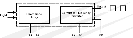
Frequency of Color Sensor TCS230 with Microcontroller AT89S51
The TCS230 programmable color light-to-frequency converter
combines configurable silicon photodiodes and a current-to-frequency
converter on single monolithic CMOS integrated circuit. The output is
a square wave (50% duty cycle) with frequency directly proportional
to light intensity (irradiance). The full-scale output frequency can
be scaled by one of three preset values via two control input pins.
Digital inputs and digital output allow direct interface to a microcontroller
or other logic circuitry. Output enable (OE) places the output in the
high-impedance state for multiple-unit sharing of a microcontroller
input line.
The light-to-frequency converter reads an 8 x 8 array of photodiodes.
Sixteen photodiodes have blue filters, 16 photodiodes have green filters,
16 photodiodes have red filters, and 16 photodiodes are clear with no
filters. The four types (colors) of photodiodes are interdigitated to
minimize the effect of non-uniformity of incident irradiance. All 16
photodiodes of the same color are connected in parallel and which type
of photodiode the device uses during operation is pin-selectable. Photodiodes
are 120 mm x 120 mm in size and are on 144-mm centers.
Functional Block Diagram
Terminal Function
Terminal
Name |
No |
I/O |
Description |
| GND |
4 |
- |
Power supply ground. All voltages are referenced to GND. |
| OE |
3 |
In |
Enable for fo (active low). |
| OUT |
6 |
Out |
Output frequency (fo). |
| S0, S1 |
1,2 |
In |
Output frequency scaling selection inputs. |
| S2,S3 |
7,8 |
In |
Photodiode type selection inputs. |
| VDD |
5 |
- |
Supply voltage |
S0 |
S1 |
Output Frequency Scaling
( fc ) |
|
S2 |
S3 |
Photodiode Type |
L |
L |
Power Down |
L |
L |
Red |
L |
H |
2% |
L |
H |
Blue |
H |
L |
20% |
H |
L |
Clear ( No Filter ) |
H |
H |
100% |
H |
H |
Green |
APPLICATION INFORMATION
Power supply considerations
Power-supply lines must be decoupled by a 0.01-mF to 0.1-mF capacitor
with short leads mounted close to the device package.
Input interface
A low-impedance electrical connection between the device OE pin and
the device GND pin is required for improved noise immunity.
Output interface
The output of the device is designed to drive a standard TTL or CMOS
logic input over short distances. If lines greater than 12 inches are
used on the output, a buffer or line driver is recommended.
Photodiode type (color) selection
The type of photodiode (blue, green, red, or clear) used by the device
is controlled by two logic inputs, S2 and S3 (see Table 1).
Output frequency scaling
Output-frequency scaling is controlled by two logic inputs, S0 and S1.
The internal light-to-frequency converter generates a fixed-pulsewidth
pulse train. Scaling is accomplished by internally connecting the pulse-train
output of the converter to a series of frequency dividers. Divided outputs
are 50%-duty cycle square waves with relative frequency values of 100%,
20%, and 2%. Because division of the output frequency is accomplished
by counting pulses of the principal internal frequency, the final-output
period represents an average of the multiple periods of the principle
frequency. The output-scaling counter registers are cleared upon the
next pulse of the principal frequency after any transition of the S0,
S1, S2, S3, and OE lines. The output goes high upon the next subsequent
pulse of the principal frequency, beginning a new valid period. This
minimizes the time delay between a change on the input lines and the
resulting new output period. The response time to an input programming
change or to an irradiance step change is one period of new frequency
plus 1 mS. The scaled output changes both the full-scale frequency and
the dark frequency by the selected scale factor. The frequency-scaling
function allows the output range to be optimized for a variety of measurement
techniques. The scaled-down outputs may be used where only a slower
frequency counter is available, such as low-cost microcontroller, or
where period measurement techniques are used.
Measuring the frequency
The choice of interface and measurement technique depends on the desired
resolution and data acquisition rate. For maximum data-acquisition rate,
period-measurement techniques are used. Output data can be collected
at a rate of twice the output frequency or one data point every microsecond
for full-scale output. Period measurement requires the use of a fast
reference clock with available resolution directly related to reference
clock rate. Output scaling can be used to increase the resolution for
a given clock rate or to maximize resolution as the light input changes.
Period measurement is used to measure rapidly varying light levels or
to make a very fast measurement of a constant light source. Maximum
resolution and accuracy may be obtained using frequency-measurement,
pulse-accumulation, or integration techniques. Frequency measurements
provide the added benefit of averaging out random- or high-frequency
variations (jitter) resulting from noise in the light signal. Resolution
is limited mainly by available counter registers and allowable measurement
time. Frequency measurement is well suited for slowly varying or constant
light levels and for reading average light levels over short periods
of time. Integration (the accumulation of pulses over a very long period
of time) can be used to measure exposure, the amount of light present
in an area over a given time period.
Comments,
questions and discussion about this topic
NEXT
|
