| 
Microcontroller Kits
Programmer
and Target 89s51
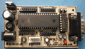
Simple
Mikrokontroller 89s51 Trainer

Standart
Mikrokontroller 89s51 Trainer

Super Mikrokontroller
Trainer 89s51
+
All Item Include
Programmer
Via USB

|
|
BACK
NEXT
1.2. Special Function Register
A Map of the on-chip memory area called the Special Function
Register (SFR) space is shown in Figure 1.2.1. Note that in the SFRs not
all of the addresses are occupied. Unoccupied addresses are not implemented
on the chip. Read accesses to these addresses will in general return random
data, and write accesses will have no effect. User software should not
write 1s to these unimplemented locations, since they may be used in other
80C51 Family derivative products to invoke new features. The functions
of the SFRs are described in the text that follows.

Figure 1.2.1. MCS-51 SFR Memory Map
Accumulator
ACC is the Accumulator register. The mnemonics for Accumulator-Specific
instructions, however, refer to the Accumulator simply as A.
B Register
The B register is used during multiply and divide operations. For other
instructions it can be treated as another scratch pad register.
Program Status Word
The PSW register contains program status information as detailed in Tabel
1.2.1
Stack Pointer
The Stack Pointer register is 8 bits wide. It is incremented before data
is stored during PUSH and CALL executions. While the stack may reside
anywhere in on-chip RAM, the Stack Pointer is initialized to 07H after
a reset. This causes the stack to begin at locations 08H.
Data Pointer
The Data Pointer (DPTR) consists of a high byte (DPH) and a low byte (DPL).
Its intended function is to hold a 16-bit address. It may be manipulated
as a 16-bit register or as two independent 8-bit registers.
Ports 0 to 3
P0, P1, P2, and P3 are the SFR latches of Ports 0, 1, 2, and 3, respectively.
Writing a one to a bit of a port SFR (P0, P1, P2, or P3) causes the corresponding
port output pin to switch high. Writing a zero causes the port output
pin to switch low. When used as an input, the external state of a port
pin will be held in the port SFR (i.e., if the external state of a pin
is low, the corresponding port SFR bit will contain a 0; if it is high,
the bit will contain a 1).
Serial Data Buffer
The Serial Buffer is actually two separate registers, a transmit buffer
and a receive buffer. When data is moved to SBUF, it goes to the transmit
buffer and is held for serial transmission. (Moving a byte to SBUF is
what initiates the transmission.) When data is moved from SBUF, it comes
from the receive buffer.
Timer Registers
Register pairs (TH0, TL0), and (TH1, TL1) are the 16-bit Counting registers
for Timer/Counters 0 and 1, respectively.
Control Register
Special Function Registers IP, IE, TMOD, TCON, SCON, and PCON contain
control and status bits for the interrupt system, the Timer/Counters,
and the serial port. They are described in later sections.
Table 1.2.1 Program Status Word
MSB |
|
LSB |
CY |
AC |
F0 |
RS1 |
RS0 |
OV |
- |
P |
BIT |
SYMBOL |
FUNCTION |
PSW.7 |
CY |
Carry flag. |
PSW.6 |
AC |
Auxilliary Carry flag. (For BCD operations.) |
PSW.5 |
F0 |
Flag 0. (Available to the user for general purposes.) |
PSW.4 |
RS1 |
Register bank select control bit 1.
Set/cleared by software to determine working register bank. (See
Note.) |
PSW.3 |
RS0 |
Register bank select control bit 0.
Set/cleared by software todetermine working register bank. (See
Note.) |
PSW.2 |
OV |
Overflow flag. |
PSW.1 |
- |
User-definable flag. |
PSW.0 |
P |
Parity flag.
Set/cleared by hardware each instruction cycle to indicate an odd/even
number of “one” bits in the Accumulator, i.e., even
parity. |
Program Status Word
The Program Status Word (PSW) contains several status bits that reflect
the current state of the CPU. The PSW, shown in Figure 10, resides in
the SFR space. It contains the Carry bit, the Auxiliary Carry (for BCD
operations), the two register bank select bits, the Overflow flag, a Parity
bit, and two user-definable status flags. The Carry bit, other than serving
the function of a Carry bit in arithmetic operations, also serves as the
“Accumulator” for a number of Boolean operations. The bits
RS0 and RS1 are used to select one of the four register banks shown in
Figure 1.7. A number of instructions refer to these RAM locations as R0
through R7. The selection of which of the four is being referred to is
made on the basis of the RS0 and RS1 at execution time.
The Parity bit reflects the number of 1s in the Accumulator:
P = 1 if the Accumulator contains an odd number of 1s, and P = 0 if
the Accumulator contains an even number of 1s. Thus the number of 1s
in the Accumulator plus P is always even. Two bits in the PSW are uncommitted
and may be used as general purpose status flags.
Comments,
questions and discussion about this topic
BACK
NEXT
|
|
|
|
